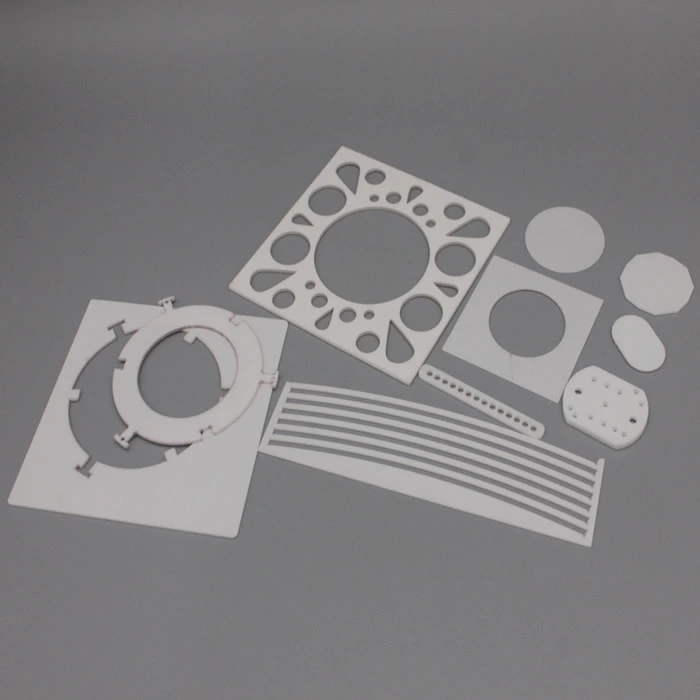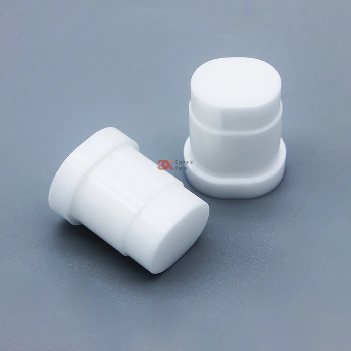
Industrial pattern of silicon carbide ceramic structural parts for photolithography
Industrial pattern of silicon carbide ceramic structural parts for photolithography
It has great advantages to use silicon carbide as the material of precision structural parts for IC key equipment such as lithography machine. However, traditional ceramic preparation processes such as grouting and dry pressing are difficult to achieve the preparation of complex components such as lithography machine workbench. To this end, China National Academy of building materials has developed a series of molding and sintering technologies to solve the localization problem of using silicon carbide materials to make such parts.
Silicon carbide ceramics have excellent properties such as high strength, high hardness, high modulus of elasticity, high specific stiffness, high thermal conductivity, low coefficient of thermal expansion and so on. It is an ideal high-performance structural material. However, when it is applied to the preparation of precision structural parts for IC key equipment such as photolithography machines with the characteristics of "large, thick, empty, thin, light and fine", there are many technical difficulties and challenges, such as how to realize hollow and closed cell structures, To achieve the goal of high lightweight and high mode; How to obtain materials with uniform microstructure and stable performance; How to realize the rapid preparation of ceramic parts with large size and complex shape structure.
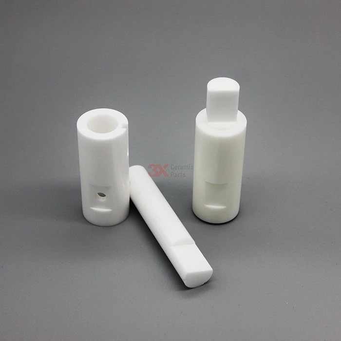
Based on the near net size molding process - gel injection molding, China National Academy of building materials has developed a process technology for preparing new large-size, complex shape and high-precision silicon carbide ceramic components. Firstly, the structural characteristics of ceramic parts are analyzed, and simple or complex molds are designed and manufactured for gel injection molding to prepare ceramic parts blank; Then, the ceramic parts are precision machined to improve the dimensional accuracy and surface finish of ceramic parts; Finally, the product is obtained by high-temperature sintering. For the hollow structure silicon carbide ceramic parts, the bonding process is used to bond the ceramic blank monomer parts to form an integral part, and then placed in the vacuum sintering furnace to sinter the designed silicon carbide ceramic parts.
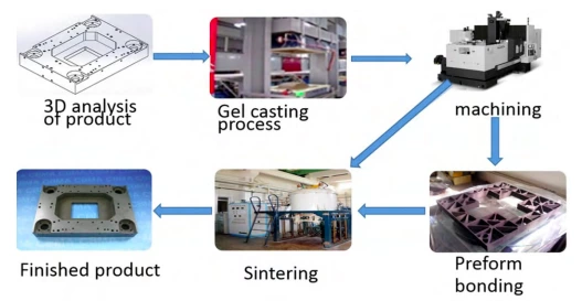
Preparation process flow chart of silicon carbide ceramic parts
The key processes in the preparation process include gel injection molding process, ceramic blank processing process and ceramic blank connection process. Among them, the gel casting process is the basis for the preparation of silicon carbide ceramic parts. This process is a fine colloidal molding process, which can realize the high strength, high uniformity and near net size molding of large-size and complex structure green bodies. It has been widely studied in the field of special ceramic material preparation. Ceramic blank processing technology can realize the rapid, low-cost and precise manufacturing of ceramic parts with complex shapes, and effectively improve the dimensional accuracy and surface finish of ceramic parts. Ceramic blank connection process can realize the preparation of hollow ceramic parts, mainly using ceramic adhesives to connect the ceramic monomer parts to obtain the whole hollow parts.
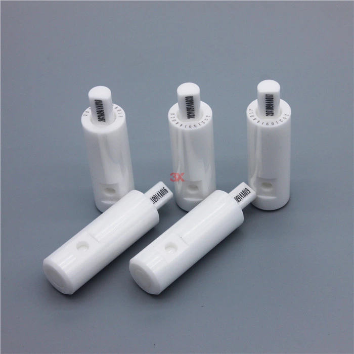
Industrial pattern of silicon carbide ceramic structural parts for photolithography
At present, the global expenditure on integrated circuit manufacturing equipment has reached US $50billion, of which ceramic structural parts account for more than 20% of the expenditure. At present, 70% of high-end silicon carbide ceramic parts for IC manufacturing equipment are monopolized by Kyocera and coorstek, and the rest are also occupied by European, American and Japanese enterprises.
Kyocera and coorstek products are characterized by a complete range of products and wide market coverage. Taking ceramic components for semiconductors as an example, the precision ceramic structural components provided by coorstek cover a series of products, such as special components for photolithography machine, special components for plasma etching equipment, special components for pvd/cvd, special components for ion implantation equipment, special components for wafer adsorption, fixed transmission, etc; Kyocera provides special ceramic parts such as lithography machine, wafer manufacturing equipment, etching machine, deposition equipment (CVD, PVD), liquid crystal panel (LCD) manufacturing equipment, etc.