Silicon carbide ceramic precision parts , inject soul into the new generation of lithography machine
Silicon carbide ceramic precision parts: inject "soul" into the new generation of lithography machine
The key equipment of integrated circuit represented by lithography machine is the product of high integration of modern technology. Its design and manufacturing process can reflect the highest level in many related scientific fields, including material science and engineering, machining and so on.
For the discipline of materials science and engineering, the key equipment of integrated circuit manufacturing requires that the component materials have the characteristics of light weight, high strength, high thermal conductivity and low thermal expansion coefficient, and are dense and uniform without defects; For the mechanical processing discipline, the key equipment of integrated circuit manufacturing requires high dimensional accuracy and dimensional stability of components to ensure the ultra precision movement and control of the equipment.
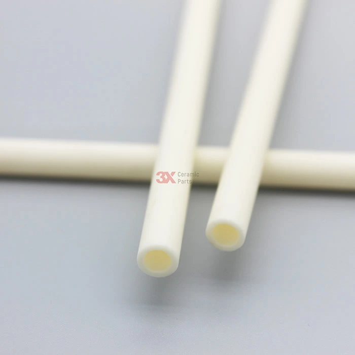
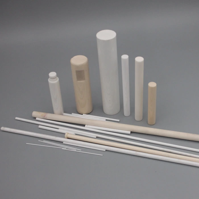
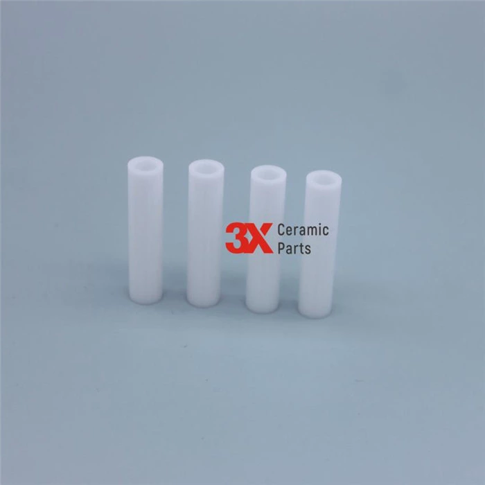
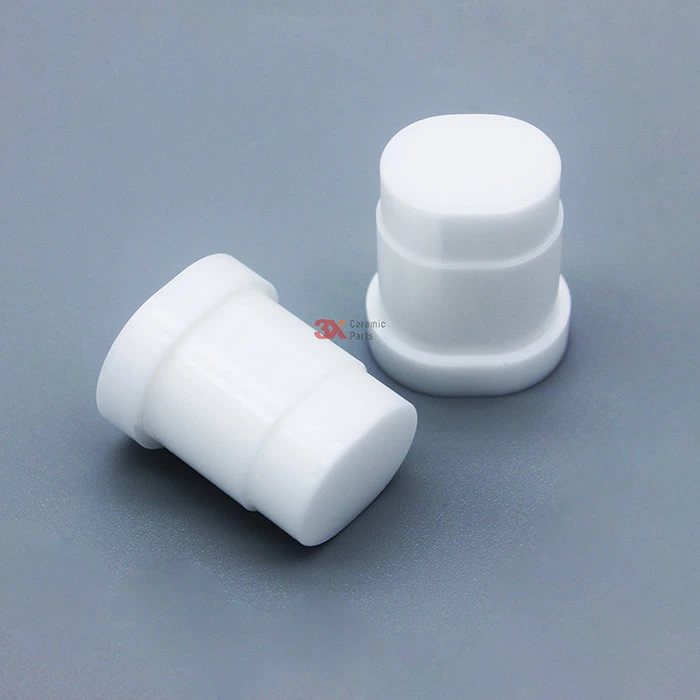
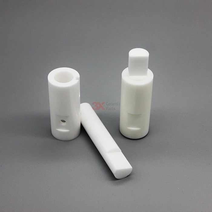
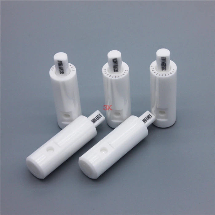
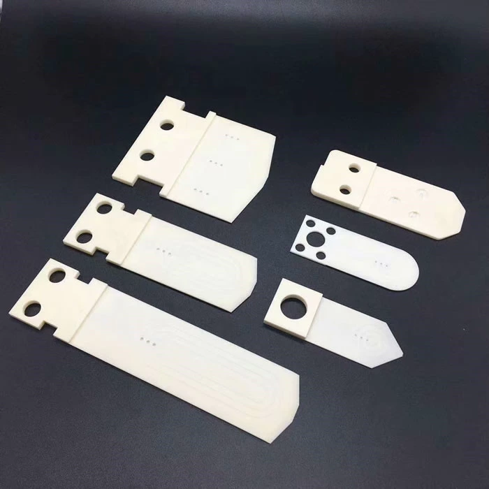
Preferred material for precision parts of lithography machine -- silicon carbide ceramics
Silicon carbide ceramics have high elastic modulus and specific stiffness, are not easy to deform, and have high thermal conductivity and low coefficient of thermal expansion, and high thermal stability. Therefore, silicon carbide ceramics is an excellent structural material, which has been widely used in aviation, aerospace, petrochemical industry, machinery manufacturing, nuclear industry, microelectronic industry and other fields. However, silicon carbide is a covalent compound with strong Si-C bond, which has extremely high hardness and significant brittleness, so it is difficult to precision machining; In addition, silicon carbide has a high melting point, which makes it difficult to achieve dense, near net size sintering.
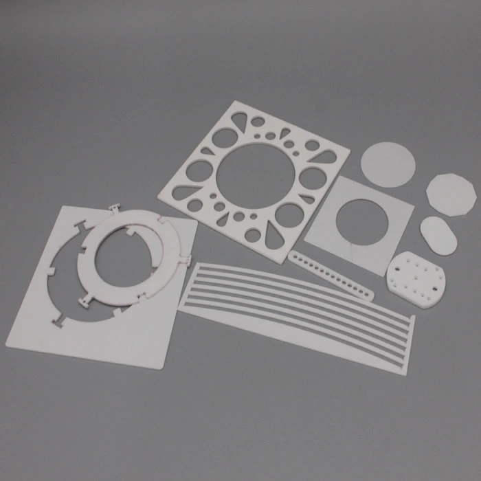
Therefore, it is difficult to prepare precision silicon carbide structural parts with large size and complex special-shaped hollow structure, which limits the wide application of silicon carbide ceramics in high-end equipment manufacturing fields such as integrated circuits. At present, only a few enterprises in a few developed countries such as Japan and the United States (such as Kyocera in Japan, coorstek in the United States, etc.) have successfully applied silicon carbide ceramic materials to key equipment for integrated circuit manufacturing, such as silicon carbide worktable for lithography, guide rail, reflector, ceramic chuck, arm, etc.
Application of silicon carbide ceramic structure in lithography machine
The key technologies and equipment of integrated circuit manufacturing mainly include lithography technology and lithography equipment, film growth technology and equipment, chemical mechanical polishing technology and equipment, high-density post packaging technology and equipment, etc., all of which involve high-efficiency, high-precision, high-stability motion control technology and driving technology, and put forward high requirements for the accuracy of structural parts and the performance of structural materials.
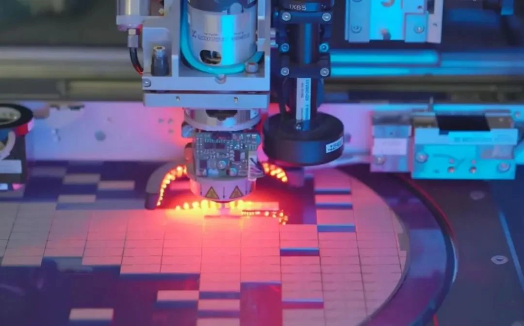
● silicon carbide worktable
Take the worktable in the lithography machine as an example. The worktable is mainly responsible for completing the exposure movement, and requires high-speed, large stroke and six degrees of freedom nano ultra precision movement. For example, for the lithography machine with 100nm resolution, 33nm nesting accuracy and 10nm linewidth, the worktable positioning accuracy is required to reach 10nm, the mask silicon wafer simultaneous step and scanning speed are 150nm/s and 120nm/s respectively, and the mask scanning speed is close to 500nm / s, And the workpiece table is required to have very high motion accuracy and stability.
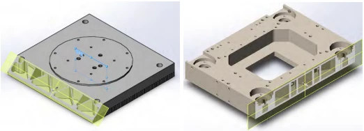
Schematic diagram of workpiece table and inching table (local section)
Generally speaking, the workpiece table structure for lithography machine shall meet the following requirements:
① High lightweight: in order to reduce the motion inertia, reduce the motor load, and improve the motion efficiency, positioning accuracy and stability, lightweight structural design is widely used for structural parts, with a lightweight rate of 60% - 80%, up to 90%;
② High form and position accuracy: in order to achieve high-precision movement and positioning, structural members are required to have extremely high form and position accuracy, and the flatness, parallelism and perpendicularity are required to be less than 1 μ m. The shape and position accuracy shall be less than 5 μ m;
③ High dimensional stability: in order to achieve high-precision movement and positioning, structural members are required to have high dimensional stability, which is not easy to produce strain, and high thermal conductivity, low thermal expansion coefficient, which is not easy to produce large dimensional deformation;
④ Clean and pollution-free: structural members are required to have extremely low friction coefficient, small kinetic energy loss during movement, and no pollution of grinding particles.
● silicon carbide ceramic square mirror
The key components in the key equipment of integrated circuits such as lithography machine have the characteristics of complex shape, complex overall dimension and hollow lightweight structure, so it is difficult to prepare such silicon carbide ceramic components. At present, the international mainstream integrated circuit equipment manufacturers, such as ASML in the Netherlands, Nikon and Canon in Japan, use a large number of microcrystalline glass, cordierite and other materials to prepare the core component of the lithography machine - square mirror, and use silicon carbide ceramics to prepare other simple shape high-performance structural components. However, the experts of China Academy of building materials science have adopted proprietary preparation technology to realize the preparation of large-size, complex shape, highly lightweight, fully enclosed silicon carbide ceramic square mirrors and other structural and functional optical components for lithography.
● silicon carbide mask film
At a semiconductor exchange event in South Korea a few days ago, myoungkuylee, ASML's South Korean Marketing Manager, revealed that he would start supplying films with a light transmittance of more than 90% to improve the efficiency of EUV lithography machines. ASML first developed the mask film in 2016, when the light transmittance was 78%. Then in 2018, the light transmittance of the film increased to 80% and 85% in 2020.
The film is used to protect the mask from pollution, and the unit price is about 26000 US dollars (about 167800 yuan). In addition, South Korean enterprises FST and s&stech are also developing the films required for EUV lithography. FST had expected to supply silicon carbide films with 90% light transmittance in the first half of the year.